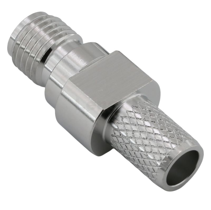
High-frequency board design demands intense attention to detail. Every component transition directly impacts your overall signal integrity. Substrate thickness and edge-mount components share a highly critical relationship. A mismatched end launch connector creates severe air gaps. It also introduces sudden impedance discontinuities and severe mechanical instability. Engineers transitioning from early prototyping to a final Bill of Materials must choose wisely. Selecting the appropriate edge component ensures a highly seamless transition. You move smoothly from external test equipment to the bare board. We provide an objective, engineering-focused framework below. You will learn exactly how to match your board thickness perfectly. Our guide helps minimize VSWR degradation throughout your system. It also streamlines your component procurement process for production runs.
Key Takeaways
Standard Compatibility: Most commercial off-the-shelf (COTS) end launch connectors are optimized for standard PCB thicknesses: 0.031" (0.8mm), 0.062" (1.6mm), and 0.093" (2.4mm).
Signal Integrity First: Precision matching at the edge launch point is non-negotiable for frequencies up to 18 GHz to maintain a 50-ohm impedance.
Mechanical Realities: Thicker boards (e.g., 100mil/2.54mm) require specialized connector geometries to prevent mounting stress when mating with an SMA cable connector.
Evaluation Focus: Base your final selection on CAD model availability, verified VSWR test data, and substrate tolerance margins.
The Engineering Problem: Why PCB Thickness Dictates Connector Selection
Impedance continuity acts as the foundation of high-frequency design. The center pin and ground legs must align perfectly. They connect directly to your microstrip or coplanar waveguide (CPW). Perfect alignment prevents dangerous capacitive and inductive spikes. Poor alignment distorts the electromagnetic field lines abruptly. These distortions reflect power back to your source immediately. This reflection ruins your signal clarity entirely. Engineers often overlook the physical alignment zone. They assume trace width alone dictates overall impedance. The physical transition zone remains equally vital to maintain a strict 50-ohm match.
Air gap risks present another massive challenge. Imagine mounting a component designed for a 0.093-inch board onto a thinner 0.062-inch substrate. The resulting physical gap requires massive solder bridging. Solder behaves poorly as a controlled dielectric medium. Large solder blobs degrade high-frequency performance drastically. They create localized parasitic capacitance immediately. They also alter the characteristic impedance along the launch path. A tightly matched gap prevents these issues. It keeps the electromagnetic fields tightly constrained.
Mechanical stress introduces a major physical failure mode. We often call this the leverage effect. An improperly fitted SMA connector for PCB application acts as a mechanical lever. Heavy RF cables apply downward tension continuously. This leverage forces the connector legs against your fragile substrate. You will eventually discover cracked solder joints. Trace delamination often follows these cracks. The entire pad might rip off the board under sheer stress. Proper gap matching eliminates this dangerous pivoting action.
Standard PCB Thicknesses and End Launch Capabilities
Industry standards heavily favor specific board dimensions. The 0.031" (0.8mm) and 0.062" (1.6mm) sizes dominate the modern electronics market. They represent the established baseline everywhere.
Most FR4 materials utilize these exact depths.
High-frequency Rogers laminates also favor these specific thicknesses.
Suppliers stock these standard sizes heavily worldwide.
You benefit from high availability globally.
You also enjoy much lower procurement lead times. Designers default to these sizes for rapid prototyping. They ensure a fast transition from simulation to physical testing.
Some advanced designs demand thicker boards. These depths range from 0.093" (2.4mm) to 100mil (2.54mm). High-power handling circuits demand thicker substrates strictly for thermal dissipation. Multi-layer complex stackups also require extra physical depth. However, commercial off-the-shelf (COTS) edge mounts remain limited here. You face restricted options for these 100mil boards. You must review specific manufacturer datasheets carefully. Do not assume universal availability for thick boards. Custom orders often become necessary.
Tolerance margins complicate the selection process further. Boards carry inherent manufacturing tolerances. A standard "0.062 inch" board usually fluctuates by ±10%. Your chosen component must feature a forgiving mounting gap. It must accommodate this maximum tolerance safely. It should fit snugly without excessive physical play. Loose fits cause the mechanical leverage issues mentioned earlier. Tight fits can crush the delicate substrate layers during assembly.
PCB Thickness vs. Connector Availability Matrix
Board Thickness (Inches)
Board Thickness (mm)
Common Material Applications
COTS Availability Status
0.031"
0.8 mm
Rogers/PTFE high-frequency boards
Very High
0.062"
1.6 mm
Standard FR4 / Mixed dielectrics
Very High
0.093"
2.4 mm
Multi-layer RF stackups
Moderate
0.100"
2.54 mm
High-power / Rigid backplanes
Low (Often Custom)
Evaluating RF Performance at the Transition Point
VSWR and Return Loss define your acceptable loss criteria. A correctly sized end launch component supports very high operational frequencies. You should achieve operation up to 18 GHz easily. It must do this while ensuring minimal reflection. Mismatched gaps cause harsh electrical reflections. Reflections increase your VSWR dramatically. High VSWR means wasted transmitter power. It also means distorted receiver sensitivity. You need smooth energy transfer across the physical boundary. Proper thickness matching secures this energy transfer.
Trace geometry alignment requires careful mathematical modeling. The physical transition from the center pin to the PCB trace matters greatly. Your pin diameter must correlate directly with your trace width. Trace width is inherently tied to the specific dielectric thickness. You manipulate trace width to maintain a strict 50-ohm impedance. Thick center pins sitting on extremely narrow traces create severe mismatch. The resulting step change in width alters the fringing capacitance. This capacitance spike degrades high-frequency performance instantly.
Test board deployment tests your design rigor perfectly. These edge transitions function as highly critical interfaces. They link a diagnostic SMA cable connector directly to the device under test (DUT). Poor interface transitions mask true DUT performance. You cannot differentiate connector loss from actual circuit loss. Engineers waste hours troubleshooting phantom circuit bugs. Often, the poorly matched edge launch causes the exact failure. A matched transition guarantees accurate diagnostic measurements.
Implementation Risks and Mounting Considerations
Soldering heavy components presents a serious thermal mass challenge. Ground legs utilize dense brass or heavy stainless steel. Heating these massive legs takes substantial thermal energy. Your soldering iron must deliver prolonged heat. However, pushing too much heat damages thinner substrates. A 0.031" board melts or warps quickly under extreme heat. You risk burning the FR4 resin. You might even melt the delicate dielectric core. You must balance your thermal profile carefully. Pre-heating the board often prevents sudden thermal shock.
Many technicians rely on dangerous gap filling habits. We must debunk this widespread myth immediately. Solder cannot simply "fill the gap" successfully. Excess solder alters the local dielectric constant permanently. It ruins high-frequency performance completely. Solder is meant strictly for electrical bonding. It is never designed for structural shimming. A massive fillet of solder creates unwanted inductance. It changes the carefully calculated 50-ohm impedance curve.
Footprint design prevents costly physical assembly errors. You need a highly customized PCB footprint design. Base this footprint exactly on the 3D step model. Get this model directly from the connector manufacturer. Never rely on generic software library footprints. Generic footprints ignore specific leg widths. They also ignore unique gap depths. Precision footprint design guarantees a tight mechanical fit. It simplifies the final assembly process immensely.
Shortlisting Logic: Selecting Your SMA Connector
Finalize the Stackup: Do not select your SMA Connector too early. Wait until the PCB manufacturer confirms the final pressed thickness. This final number includes copper plating. It also includes the outer soldermask layers. These microscopic additions change the final gap requirement.
COTS vs. Custom Evaluation: Evaluate your specific project needs objectively. A standard 0.062" or 0.093" model often suffices. Sometimes a custom gap requirement justifies higher tooling costs. Weigh these upfront costs against longer lead times. Prototyping usually favors standard off-the-shelf options.
Verify CAD and Test Data: Only shortlist highly transparent suppliers. They must provide easily downloadable 3D CAD models. They must also share empirical VSWR and Insertion Loss test data. Ensure this published data matches your specific gap size. Never accept generic data for precision RF applications.
Mating Cycle Requirements: Assess your mechanical durability needs thoroughly. Ensure the internal plating matches your expected mating cycles. Gold over nickel offers excellent longevity. Body materials matter greatly too. Stainless steel survives far more cycles than standard brass. Brass bodies wear down quickly in harsh test environments.
Conclusion
Forcing a mismatched end launch component onto a board compromises everything. It destroys both mechanical reliability and RF signal integrity. You cannot fix physical mismatch using software calibrations. Take the time to match these critical parameters exactly. A snug fit ensures predictable impedance curves across all frequencies.
Pull your exact PCB stackup report today. Download the corresponding 3D models from your chosen supplier. Import them into your CAD environment. Verify the impedance matching inside your preferred RF simulation software. Do all this completely before you place any sample orders.
FAQ
Q: Can I use a 0.062" end launch SMA connector on a thinner 0.031" PCB?
A: Mechanically possible but electrically compromised. It requires excessive solder, causing impedance mismatch. It is highly recommended to use a connector specifically gapped for 0.031". Excess solder alters the local dielectric constant and degrades high-frequency performance.
Q: What is the maximum frequency an edge mount SMA connector can handle?
A: High-quality, properly thickness-matched SMA connectors typically support up to 18 GHz, assuming proper PCB trace design and a clean transition. Precise gap matching minimizes VSWR and reflection losses at these upper frequencies.
Q: How do I handle non-standard board thicknesses (e.g., 100mil / 2.54mm)?
A: You must source specific 0.093" or larger gap connectors. If COTS options are unavailable, consider top-mount (surface mount) alternatives, or contact suppliers for customized gap configurations to ensure a stress-free fit.
Q: Does the weight of the SMA cable connector affect the edge mount choice?
A: Yes. Heavy cables require thick, stable boards and connectors with broad ground legs to distribute mechanical strain away from the fragile signal trace. A loose fit acts as a lever and causes cracked solder joints.
Our company, Zhejiang LenoRF Industry co. LTD, occupies an area of 30 hectares and is equipped with world class equipment to make millimeter wave connectors and phase stable cables. We specialize in coaxial connectors, cable assembly, and passive devices. Our current products are the latest millimeter wave connector and phase stable cable on the market.