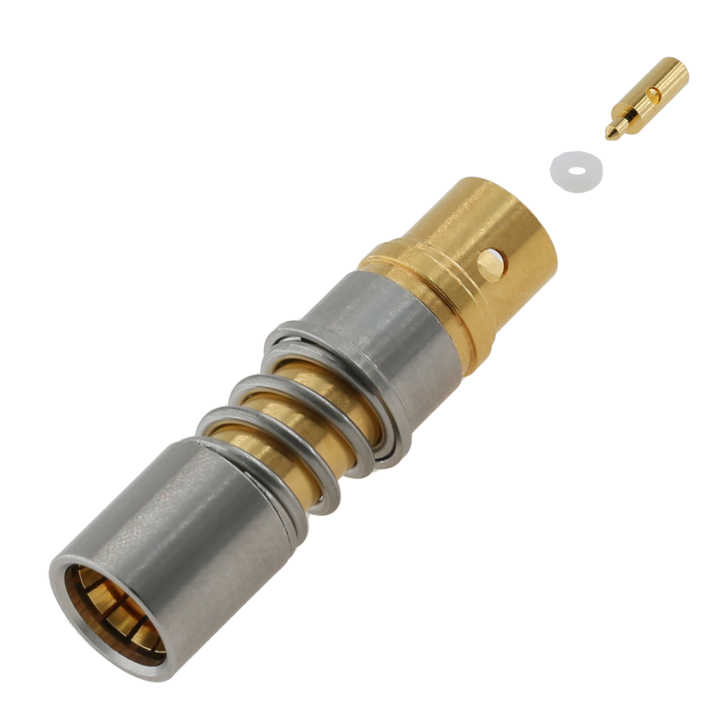
Modern hardware engineering frequently feels like an ongoing paradox. You must cram increasingly complex radio circuits into vanishingly small physical spaces. Engineers face a relentless core conflict every day. They must balance shrinking printed circuit board real estate against the strict mechanical demands of a modern system. They also must meet stringent signal integrity requirements for high-frequency data transmission. You cannot simply treat the selection of an RF connector for PCB integration as a mere mechanical afterthought. It acts as a highly critical factor directly influencing overall circuit performance. The right choice optimizes insertion loss, maintains precise impedance matching, and guarantees a high manufacturing yield. A poorly chosen physical mount can completely derail an otherwise perfect layout. We will systematically evaluate the four primary mounting styles: Surface Mount (SMD), Edge-Mount, Through-Hole, and Solderless Compression. We evaluate them strictly based on verifiable physical metrics and electrical trade-offs. You will learn how to weigh these layout choices properly. Our ultimate goal is to help you confidently select the right configuration to satisfy both your tight spatial boundaries and strict frequency constraints.
Key Takeaways
Surface Mount (SMD) offers the smallest footprint (e.g., U.FL/W.FL microminiature series) but sacrifices mechanical retention force.
Edge Mount configurations are optimal for strict Z-axis (height) constraints and parallel board-to-board routing.
Through-Hole (TH) provides superior mechanical anchoring for heavier cables but consumes valuable multi-layer routing space.
Solderless Compression is emerging as a viable alternative for high-frequency testing and modularity, eliminating reflow thermal stress.
Connector selection must align with expected mating cycles, automated assembly capabilities, and target frequency bands.
The Design Challenge: Real Estate vs. Signal Integrity
The concept of a compact board changes every year. Modern contexts redefine spatial limitations constantly. You see this clearly in modern IoT wearables. Designers measure available space in mere fractions of a millimeter. We also see it in modern 5G communications modules. These demand incredibly high-density radio frequency front-ends. When dealing with standard FR4 substrates, space is even tighter. Designing for these compact constraints forces difficult decisions daily.
Minimizing the footprint of a coaxial RF connector often introduces hidden vulnerabilities. Engineers frequently face a harsh mechanical versus electrical trade-off. A tiny surface pad reduces the overall mechanical stability. It makes the joint highly susceptible to sheer stress during assembly or handling. You might also experience a drastically reduced mating life. A micro-component simply cannot survive hundreds of physical insertion cycles without degrading.
Furthermore, the mounting pad geometry directly impacts signal integrity. Physical metal pads generate capacitive and inductive parasitics. A massive solder pad creates excess ground capacitance. It lowers the local impedance well below the standard 50-ohm target. Conversely, a too-narrow trace transition adds unwanted series inductance. You must maintain tight impedance control exactly at the transition point. Any physical mismatch causes signal reflections. It degrades your return loss heavily. We must carefully balance physical ruggedness against these parasitic effects to maintain optimal signal clarity.
Surface Mount (SMD): The Ultraminiature Baseline
Primary use cases for surface mount designs involve high-volume production. They excel in low-profile consumer devices. These manufacturing environments require rapid automated pick-and-place assembly. Automated pick-and-place assembly requires components to sit completely flat on the bare board surface. SMD components eliminate the need for manual insertion steps entirely. Factories feed them using standard tape and reel packaging. We focus frequently on microminiature and ultraminiature standard form factors here. You will often encounter industry-standard series like U.FL, W.FL, or MHF. These tiny components provide a reliable baseline for compact modules.
These form factors present specific implementation realities. Consider the significant pros first:
They consume truly minimal board space.
They require zero drilled holes through the substrate.
You easily preserve your internal routing layers for other critical signals.
However, you must acknowledge the physical risks:
They exhibit notably weak mechanical shear strength.
The copper pads remain prone to lifting or delamination.
Attached cables subjected to sudden pull forces easily rip the pad apart. A technician might accidentally yank a test cable. This action rips the copper trace completely off the FR4 substrate.
Smart designers implement reliable mitigation strategies. You often require secondary strain relief methods. Engineers frequently use epoxy potting compounds around the component base. You might also design physical cable routing channels into the plastic enclosure. These channels restrict wire movement before stress reaches the fragile junction.
Edge Mount and Right-Angle Configurations: Managing Z-Axis Constraints
Many modern enclosures impose strict height limits on designers. You might design a slim router or a stacked multi-board module. Edge mount and right-angle configurations shine brightly in these exact scenarios. They provide optimal solutions for parallel panel-to-PCB connections. You often see them bridging gaps between stacked PCIe cards.
The structural mechanics differ greatly from top-mounted SMD varieties. Straddle-mount or edge-mount styles literally slide over the board edge. They utilize the physical board thickness for added mechanical stability. These side grips distribute physical stress laterally away from delicate solder joints. This approach proves much stronger than relying solely on surface adhesion. It anchors the component securely against side-to-side torsion.
Signal path efficiency is another major benefit here. We often use a coplanar waveguide transition for edge-mounted setups. Edge mounting offers exceptionally clean signal transitions. You achieve a significantly lower Voltage Standing Wave Ratio (VSWR) at high frequencies. Keeping the center pin precisely inline with the trace minimizes right-angle signal reflections. The signal flows straight into the device without bouncing.
However, you must accept certain layout limitations. These components require dedicated real estate right along the board perimeter. This positioning heavily complicates panelization strategies during mass production. Factories usually require edge rails for conveyor belt transport. You lose valuable edge space normally reserved for V-scoring lines, mouse bites, or structural mounting screws. Routing around the PCB perimeter becomes highly congested.
Through-Hole (TH) vs. Solderless Compression
Through-Hole (TH) solutions remain a staple for heavy-duty environments. You use them when applications require large external antennas. They seamlessly support thick, rigid cables. Standard SMA components frequently utilize four TH posts for strong mechanical anchoring around a central signal pin. They endure incredible physical abuse.
Yet, this mechanical strength exacts a high electrical cost. Drill holes inherently create vertical capacitive stubs. These Plated Through Hole (PTH) stubs severely degrade high-frequency signals. They act like tiny internal antennas radiating energy downward into the board layers. Furthermore, TH pins consume all layers situated directly beneath the footprint. You lose crucial routing channels across multiple internal ground planes. Engineers must utilize precise back-drilling techniques to remove the unused stub portion.
Solderless compression mounting provides a fascinating niche alternative. The mechanism relies purely on downward mechanical pressure. You use precisely torqued screws to compress the RF Connector directly against the top trace. Solderless mounts excel in the 40GHz to 110GHz range.
Advantages of solderless compression:
It generates zero thermal stress since there is no solder reflow process.
It protects highly sensitive, high-frequency dielectric materials from heat damage.
It provides incredible reusability for expensive prototyping and test boards. You can move the part from board to board effortlessly.
Drawbacks to consider:
The initial hardware unit cost is notably higher than standard types.
It requires strictly enforced, precise torque specifications during assembly.
Decision Matrix: How to Shortlist Your RF Connector
We map these mounting styles directly to their functional frequency limits. You must carefully match the physical footprint to your target bandwidth. Standard SMD options typically perform adequately up to 6GHz. Above this range, component parasitics become highly problematic. You might need specialized compression mounts for mmWave or sub-THz applications. A component rated for 2.4GHz Wi-Fi will fail miserably in a 40GHz radar system. It will exhibit a massive Voltage Standing Wave Ratio.
You must evaluate your expected mating cycles and retention force. Determine if the junction serves as a "set-and-forget" internal link. An internal U.FL component typically survives 30 to 50 cycles maximum. Conversely, an external user-facing SMA port easily withstands 500 or more insertion cycles. Match the ruggedness to the user's expected interaction level.
Assess the overall assembly flow and manufacturing yield. SMD parts support rapid automated assembly flawlessly. You buy them cheaply on tape and reel. Through-hole components often demand secondary wave soldering steps. Sometimes they even require costly manual soldering processes. Both choices directly impact your production timeline and final defect rates.
Finally, consider physical compliance and environmental stress factors. Vibration and mechanical shock dictate strict layout rules. Standard SMD pads often fail MIL-STD-810 or rigorous automotive shock tests. The constant vibration work-hardens the solder joint until it cracks. You must provide structural reinforcement if you deploy surface mount parts into harsh field environments.
Mounting Style Comparison Chart
Mounting Style
Ideal Frequency Range
Mechanical Strength
Assembly Method
Key Use Case
Surface Mount (SMD)
DC to 6 GHz
Low
Automated Pick & Place
Internal compact IoT modules
Edge Mount
DC to 40+ GHz
Medium to High
Automated / Manual Reflow
Low-profile parallel routing
Through-Hole (TH)
DC to 6 GHz
Very High
Wave Soldering / Manual
Heavy cables, rugged devices
Solderless Compression
Up to 110 GHz
High (Torque dependent)
Manual Screw Assembly
High-frequency test boards
Conclusion
Engineers must recognize there is no universal "best" mounting style. You only find the correct mechanical fit for your specific constraints. Every hardware project balances electrical bandwidth limits against harsh spatial realities. A mounting choice always dictates downstream signal integrity.
We strongly advise you to simulate the junction transition carefully. Always use reputable 3D electromagnetic solvers before you finalize any layout. A tiny pad geometry tweak can drastically improve your overall impedance matching. Small physical adjustments yield massive electrical performance gains.
Take proactive action early in your design phase. Reach out directly to vendors. We recommend requesting STEP models and accurate S-parameter data from manufacturers immediately. You can then validate the exact mounting footprint in your specific EDA tools. This extra verification step effectively prevents costly board respins.
FAQ
Q: How does a PCB RF connector compare to a direct solder cable connection?
A: Connectors introduce measurable insertion loss and component cost. However, they allow for excellent modularity and easier testing during production. Direct soldering saves physical space and money. Unfortunately, it makes rework highly destructive and severely complicates field repairs.
Q: What is the best RF connector mounting style for a PCB-to-panel assembly?
A: Edge mount or right-angle bulkhead configurations are typically preferred. They neatly align the physical mechanical strain with the sturdy outer chassis. This approach pulls damaging torque away from the fragile surface pads, preventing copper delamination.
Q: Do through-hole RF connectors ruin high-frequency signals?
A: Not necessarily, but they require careful design. The via stub created by the through-hole pin acts as a parasitic capacitor. You must utilize precise back-drilling techniques or specialized via-in-pad designs to maintain strict impedance matching at higher frequencies, typically above 6GHz.
Our company, Zhejiang LenoRF Industry co. LTD, occupies an area of 30 hectares and is equipped with world class equipment to make millimeter wave connectors and phase stable cables. We specialize in coaxial connectors, cable assembly, and passive devices. Our current products are the latest millimeter wave connector and phase stable cable on the market.