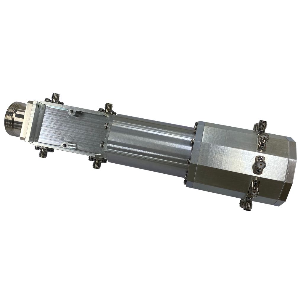
The operational success of high-frequency RF systems, including radar, electronic warfare, and satellite communications, relies entirely on the efficiency and reliability of the passive and active networks surrounding the amplification stage. While engineering teams often focus heavily on the active transistors—such as GaN or GaAs devices—the reality is that sub-optimal selection of peripheral components leads to compounding insertion losses, thermal bottlenecks, and severe phase imbalances. These issues degrade system range and frequently result in catastrophic amplifier failure.
To prevent these failures, engineers must adopt a rigorous, specification-driven approach to evaluating and selecting microwave power amplifier components. Proper component selection ensures strict impedance matching, maintains pristine signal integrity, and guarantees thermal stability across the entire required bandwidth. By prioritizing the passive network architecture, you protect the active stages and maximize the total RF output power delivered to the antenna.
System-Level Efficiency: The choice of power combiner and RF power divider directly dictates the overall efficiency of the amplifier array; even fractional decibel insertion losses scale detrimentally in high-power applications.
Isolation is Critical: High isolation in directional couplers and splitters is non-negotiable to prevent reflected power from damaging sensitive upstream active components.
Thermal and Footprint Realities: Balancing the physical footprint (surface mount vs. connectorized/monolithic) with thermal dissipation requirements is the primary trade-off in modern solid-state power amplifier (SSPA) design.
Precision Monitoring: Integrating the correct RF detector ensures accurate closed-loop power control, requiring strict evaluation of dynamic range and temperature stability.
Defining Success Criteria for Microwave Power Amplifier Components
Modern power amplifier networks operate under extreme and unforgiving demands. The industry has seen a massive shift toward wider bandwidths, with systems frequently required to operate across multi-octave bands such as 0.5 to 26.5 GHz. Simultaneously, power densities are climbing rapidly. The adoption of Gallium Nitride (GaN) and Gallium Arsenide (GaAs) technologies allows engineers to push significantly more watts through much smaller physical footprints. GaN devices, for instance, operate at higher drain voltages (typically 28V to 50V), which changes the impedance matching requirements at the board level. This high-density environment leaves zero margin for error in passive network design. If the peripheral components cannot handle the thermal load or maintain phase alignment, the entire amplifier array will underperform or self-destruct.
You must evaluate these components across strict, quantifiable metrics. Voltage Standing Wave Ratio (VSWR) dictates how well the component matches the system impedance, directly impacting return loss. Insertion loss measures the RF energy wasted as heat as the signal passes through the component. Amplitude and phase balance are mandatory when feeding multiple amplifier modules; any deviation ensures the modules will not operate in unison. Finally, power handling capabilities must be scrutinized under both Continuous Wave (CW) and pulsed conditions. Peak power spikes in pulsed radar applications can easily arc across internal gaps if the component is only rated for average CW power.
These components do not operate in a vacuum. They must function cohesively to maintain a strict 50-ohm impedance match across the entire operating frequency band. Any impedance mismatch creates signal reflections. Reflected energy travels backward through the system, creating standing waves that generate localized voltage spikes. These spikes routinely destroy sensitive amplifier gate structures. Therefore, your passive network must absorb or redirect these reflections to protect the active devices.
Evaluation Metric
Primary Impact on System
Acceptable Baseline (Typical)
VSWR (Return Loss)
Impedance matching and reflection mitigation
< 1.3:1 (15 dB Return Loss)
Insertion Loss
Thermal generation and overall efficiency
< 0.5 dB per stage
Phase Balance
Combining efficiency in parallel arrays
± 2 to 5 degrees
Amplitude Balance
Linearity and saturation prevention
± 0.2 dB
Evaluating RF Power Dividers for Signal Distribution
Splitting microwave signals prior to amplification requires specific architectural choices based on bandwidth, isolation, and physical space constraints. The two primary architectures dominate this space, each with distinct advantages and limitations.
Wilkinson power dividers remain the industry standard for applications requiring high isolation and matched output ports. They utilize quarter-wave transformers to achieve impedance matching, making them highly efficient at their specific center frequency. The internal isolation resistor (typically 100 ohms in a 50-ohm system) absorbs out-of-phase signals, providing excellent port-to-port isolation. However, their reliance on quarter-wave lengths means their bandwidth is inherently limited. Furthermore, at lower frequencies (e.g., VHF or UHF bands), the physical length of the quarter-wave trace becomes a major size constraint on the printed circuit board (PCB).
Resistive power dividers offer a completely different value proposition. You choose these when ultra-wideband performance is prioritized over insertion loss. A standard 2-way resistive split inherently loses 6 dB of signal power, as half the energy burns off as heat in the internal resistors. Despite this massive penalty, they offer unparalleled frequency coverage, operating from DC up to millimeter-wave frequencies with an exceptionally flat response.
Building 4-way or 8-way surface mount splitting networks requires cascading multiple 2-way dividers. When designing these networks, you must follow strict layout rules:
Maintain absolute PCB layout symmetry. Any trace length difference, even a fraction of a millimeter, creates phase skew between the output ports.
Calculate the compounding insertion loss of each stage. A 4-way Wilkinson split will inherently have more than 3 dB of loss, plus the dielectric and conductor losses of the PCB material.
Implement a pre-driver amplifier stage if the total splitting loss degrades the signal below the required input threshold of the main power amplifier array.
Engineers frequently ask if they can use an RF power divider in reverse as a combiner. The answer is yes, but with strict operational limits. When combining unequal or out-of-phase signals, the isolation resistor must absorb the difference. If the differential power exceeds the resistor's thermal rating, it will burn out, destroying the component. You must calculate the maximum expected phase and amplitude imbalance under worst-case scenarios to ensure the resistor survives.
Amplitude and phase tracking specifications directly impact the linearity and efficiency of the downstream amplifier stages. If a divider feeds four parallel amplifier modules, uneven signal distribution causes severe problems. The module receiving the strongest signal will hit compression and saturation early, generating distortion. Meanwhile, the modules receiving weaker signals operate inefficiently. This uneven power distribution drives individual amplifier transistors into premature saturation, causing thermal stress and eventual permanent damage.
Directional Couplers: Impedance Matching and Signal Sampling
A directional coupler plays a highly specific and protective role in power amplifier architecture. It samples a small, precise fraction of the main RF signal without disrupting the primary transmission path. You use this sampled signal for forward power monitoring, allowing the system telemetry to verify that the amplifier is outputting the correct power level. You also use couplers in reverse to measure reflected power returning from the antenna. This allows the system to calculate VSWR in real-time and shut down the amplifier if the antenna becomes damaged or disconnected.
Quadrature hybrid couplers are heavily utilized in balanced amplifier designs. These 90-degree hybrids (such as Lange couplers or branch-line couplers) split the input signal into two equal paths that are 90 degrees out of phase. Two identical amplifier modules boost these signals. A second hybrid coupler at the output recombines them. This architecture drastically improves the input and output match (return loss) of the overall amplifier. Any reflected power from the antenna routes directly into an isolation load on the output coupler, rather than traveling back into the amplifier transistors. Furthermore, it provides redundancy; if one amplifier stage fails, the system continues to operate at a reduced power level rather than failing completely.
When evaluating couplers, you must analyze directivity, coupling factor tolerance, and frequency response flatness. Directivity is the most critical metric for system protection. It measures the coupler's ability to distinguish between forward and reflected waves (calculated as Isolation minus Coupling). Poor directivity means the forward signal leaks into the reflected port, invalidating your VSWR measurements. If the system cannot accurately read reflected power, the protection mechanisms will fail to trigger, leaving the amplifier vulnerable to destruction.
Power Combiner Networks: Maximizing Output and Managing Heat
Aggregating power from multiple amplifier modules into a single, high-power output requires robust and thermally stable architectures. The choice of combiner dictates the physical size, thermal management strategy, and overall efficiency of the transmitter.
Corporate combiners utilize a cascading binary structure, combining two signals into one, then combining those results again in a tree-like format. This architecture is relatively easy to design and offers excellent isolation. However, it suffers heavily from compounding insertion loss. Every stage adds loss, generating heat. For high-way counts, such as 16-way or 32-way combining, the physical footprint grows massive, and the loss becomes unacceptable for high-efficiency systems.
Radial and spatial combiners solve the problems of corporate structures for high-way-count applications. These architectures combine all signals at a single central node simultaneously. They offer significantly lower insertion loss and highly compact form factors. We see heavy use of these in aerospace and defense applications leveraging Monolithic Microwave Integrated Circuit (MMIC) technologies, where space and weight are strictly limited.
Architecture Type
Primary Advantage
Primary Limitation
Best Use Case
Corporate Combiner
Easy to design, highly modular
Compounding loss, large footprint
Low-way count (2-way, 4-way)
Radial Combiner
Low loss, compact size
Complex machining, difficult to tune
High-way count (8-way, 16-way)
Spatial Combiner
Extremely high power handling
Requires free-space transition
Millimeter-wave arrays
You always trade combining efficiency for isolation. A high-power power combiner must handle catastrophic module failures gracefully. If one amplifier channel dies, its power no longer reaches the output node. Instead, the power from the surviving modules dumps into the combiner's internal isolation resistors. The combiner must safely dissipate this massive heat load without entering thermal runaway. If the isolation resistor fails, the entire combiner network will likely melt or catch fire. Engineers must size these resistors based on the worst-case failure mode, often requiring beryllium oxide (BeO) or aluminum nitride (AlN) flanged resistors bolted directly to a liquid-cooled cold plate.
Millimeter-wave frequencies introduce severe mechanical and electrical challenges. At frequencies above 30 GHz, parasitic capacitance wreaks havoc on phase alignment. Structural tolerances must be microscopic. Even a fraction of a millimeter in machining error on a radial combiner housing will severely impact phase alignment, causing destructive interference at the output node and drastically reducing the combined power.
RF Detectors: Precision Monitoring and Feedback Control
Converting RF power levels into measurable DC voltages is mandatory for system telemetry and closed-loop control. You need highly accurate components to feed data back to the system controller, allowing it to adjust gain, monitor health, and trigger safety shutdowns.
Schottky diode detectors offer incredibly fast response times. They provide a low-cost, highly effective implementation for peak power detection in pulsed radar systems. Because they react almost instantly to RF envelopes, they are ideal for tracking fast pulse edges. However, they struggle to accurately measure the true power of complex, modulated signals.
Logarithmic amplifiers, commonly known as log detectors, are required for applications demanding a wide dynamic range. They provide precise Root Mean Square (RMS) power measurement. This is absolutely mandatory for complex, high-crest-factor modulation schemes like OFDM used in modern communications. An RMS-responding RF detector measures the actual heating value of the signal, regardless of its peak-to-average ratio, ensuring accurate power reporting.
When evaluating detectors, focus strictly on temperature stability, frequency flatness, and video bandwidth. The video bandwidth determines how fast the detector's output voltage can track changes in the RF envelope. The detector must track accurately across the entire operational envelope. Measurement drift over extreme temperature variations is a critical failure point. In aerospace and defense deployments, temperatures swing wildly from freezing high altitudes to scorching desert tarmacs. You must mitigate this drift through hardware temperature compensation circuits or by implementing extensive software calibration tables during the manufacturing process.
Implementation Risks and System-Level Trade-Offs
Rigorous Vector Network Analyzer (VNA) testing is mandatory for all broadband components. You must validate the S-parameters across the full operating band using proper calibration techniques like SOLT (Short-Open-Load-Through) or TRL (Through-Reflect-Line). Phase and amplitude balance often look perfect at the center frequency but degrade sharply at the band edges. Relying on datasheet nominal values without sweeping the exact frequency range of your application will lead to severe system-level integration failures.
Thermal dissipation dictates the lifespan of your passive networks. You must evaluate your dielectric materials carefully. Substrates like PTFE (Teflon), Alumina, and Aluminum Nitride behave very differently under thermal stress. Aluminum Nitride offers excellent thermal conductivity (around 170 W/m·K) compared to standard Alumina (around 24 W/m·K), making it superior for high-power isolation resistors. More importantly, the Coefficient of Thermal Expansion (CTE) mismatch between the substrate, the copper traces, and the baseplate will tear solder joints apart under repeated thermal cycling. Selecting materials with matched CTEs is required for high-reliability systems.
Packaging choices dictate integration realities. Surface Mount Technology (SMT) components offer automated, high-volume assembly but struggle to shed heat into the PCB. Connectorized modules using SMA, N-type, or K-connectors handle massive power and offer excellent shielding. For example, N-type connectors can handle up to 300W at 10 GHz, whereas SMA connectors are typically limited to 100W. However, connectorized modules take up significant space and add weight. Monolithic structures, where the passive networks are integrated directly into the semiconductor die, offer the best high-frequency performance but carry the highest development costs.
Scaling a Solid-State Power Amplifier from a 10W module to a 1kW array changes the physics of the design. The choice of passive networks dictates this scalability. The physical limitations of isolation resistors and the size of the required heat sinks become the primary bottlenecks. You cannot simply scale up a low-power design; you must re-architect the combining network to handle the exponential increase in thermal density.
Conclusion
The performance ceiling of any microwave power amplifier is strictly dictated by the quality, precision, and thermal resilience of its peripheral components. The active transistors provide the gain, but the couplers, dividers, and combiners dictate how much of that power actually reaches the antenna safely. Ignoring the passive network guarantees system underperformance.
Component selection follows a strict logical sequence. First, define the frequency band and bandwidth. Second, determine the peak and average power requirements. Third, select the combining and dividing architecture that fits your physical space. Fourth, specify your isolation and insertion loss budgets. Finally, choose the packaging based on your thermal constraints and assembly capabilities.
To ensure successful implementation, engineering teams should execute the following steps:
Request comprehensive S-parameter data, specifically Touchstone files, from vendors to model the components in your system simulator.
Conduct rigorous thermal simulations on all high-power nodes, specifically focusing on isolation resistors under fault conditions.
Procure evaluation boards for empirical bench testing to verify phase and amplitude balance before finalizing the Bill of Materials.
Implement strict VNA testing protocols for incoming passive components to ensure lot-to-lot consistency.
FAQ
Q: What is the difference between an RF power divider and a directional coupler?
A: An RF power divider splits a signal into multiple equal-power paths, typically used to feed multiple amplifier modules simultaneously. A directional coupler samples a very small, specific fraction of the main signal for monitoring purposes, allowing the main signal to pass through with minimal disruption or loss.
Q: Can an RF power divider be used in reverse as a power combiner?
A: Yes, most power dividers are reciprocal devices. However, when combining unequal or out-of-phase signals, the internal isolation resistors must absorb the power difference. If this differential exceeds the resistor's thermal rating, the component will be destroyed.
Q: How does insertion loss in a power combiner affect overall amplifier efficiency?
A: Insertion loss converts RF energy directly into heat. If a combiner has a 1 dB insertion loss, approximately 20% of the combined RF power is wasted as heat before it reaches the antenna. This drastically reduces the total system efficiency and increases the cooling burden.
Q: Why are quadrature hybrid couplers preferred in balanced microwave power amplifiers?
A: They split the signal 90 degrees out of phase, feed two amplifiers, and recombine them. This architecture directs any reflected power from impedance mismatches into an isolation load rather than back into the active transistors, drastically improving return loss and protecting the system.
Q: What are the key specifications to look for when selecting an RF detector for power monitoring?
A: You must evaluate the dynamic range, frequency flatness, and temperature stability. For complex modulated signals, you must select an RMS-responding log detector rather than a peak-detecting Schottky diode to ensure accurate power measurement regardless of the crest factor.
Q: How do you mitigate thermal risks in high-power RF combiners?
A: You must mount the combiner to a highly conductive heat sink, use substrate materials with high thermal conductivity like Aluminum Nitride, and ensure the internal isolation resistors are rated to handle the full power of a failed amplifier channel without burning out.
Q: What is the best RF power divider architecture?
A: There is no single best architecture. Wilkinson dividers are best for narrow-band applications requiring high isolation and low loss. Resistive dividers are best for ultra-wideband applications where high insertion loss (6 dB) is acceptable in exchange for massive frequency coverage.
Our company, Zhejiang LenoRF Industry co. LTD, occupies an area of 30 hectares and is equipped with world class equipment to make millimeter wave connectors and phase stable cables. We specialize in coaxial connectors, cable assembly, and passive devices. Our current products are the latest millimeter wave connector and phase stable cable on the market.